© ASML
All investment strategies have the potential for profit and loss, capital is at risk. Past performance is not a guide to future returns.
Imagine, if you will, that progress fizzled out in the early-90s, and computer processing power stayed static rather than doubling every 18 months, as Moore’s Law predicts.
In this alternative world, basic ‘smartphones’ exist but are bulky, burn through battery life and cost a fortune. Apps such as Snapchat and Zoom never had a chance. And Apple went bust because Steve Jobs didn't release the iPod, let alone the iPhone.
Electric cars are still a rarity, and artificial intelligence never got a ‘deep learning’ boost. So forget about buying a Tesla or asking Alexa to turn on the lights. Amazon never launched its AWS cloud computing division, meaning thousands of smaller tech firms never started up nor achieved scale. Great news for Blockbuster Video, not so much for Netflix.
Thankfully, back in the real world, our ability to build chips in ever more intricate detail continues apace. Innovation and knowledge follow, making possible medical advances and energy efficiencies, among other forms of progress.
It makes a case that ASML could be the most important company in the world.
The Dutch firm creates the machines that allow computer chip manufacturers to burn complex patterns of transistor circuitry – tiny on-off switches – onto the surface of silicon wafers. The process is called lithography.
Founded in 1984 as Advanced Semiconductor Materials Lithography, ASML now has a 90 per cent market share of this market. It remains the only company capable of making the smallest transistors.
Shrinking transistors makes it possible to pack more into the same area. Computers can then perform calculations more quickly and use less energy.
ASML’s latest machines create ‘3-nanometre chips’. The designation is a marketing term rather than an accurate component measurement. But it corresponds to placing about 250 million transistors per square millimetre.

If you took the number of transistors that can fit on a British 1p coin, increased each to the length of a standard staple and then laid them end-to-end, they would stretch to the moon and back. And each of these has to be arranged precisely on a chip to create the highly complex circuitry.
One of Apple’s chips now contains more than 114 billion transistors. That’s about the same number as all the humans born since homo sapiens evolved over 190,000 years ago.
It marks a significant advance on Intel’s first Pentium processor back in 1993, which contained about 3.1 million transistors. And that was a giant leap ahead of the firm’s first microprocessor, the 4004, which had just 2,300.
This is what exponential growth looks like in action, and ASML’s ‘EUV’ technology is preventing it from sputtering out.
What is EUV?
ASML leads the lithography field by manufacturing the only machines that use extreme ultraviolet (EUV) light.
EUV wavelengths belong to a top tier of the electromagnetic spectrum and are normally found only in outer space. They deliver the equivalent effect to using a sharper scalpel when imprinting chip designs onto silicon than is possible using deep ultraviolet (DUV) light.

ASML wasn’t the first company to apply EUV to lithography – Japan’s NTT showed off the first demo device back in 1986. But the Eindhoven-based firm solved the challenges required to maintain precision at high volume, allowing its clients to start mass producing 7nm-class chips in 2019, 5nm in 2020 and 4nm in 2022.
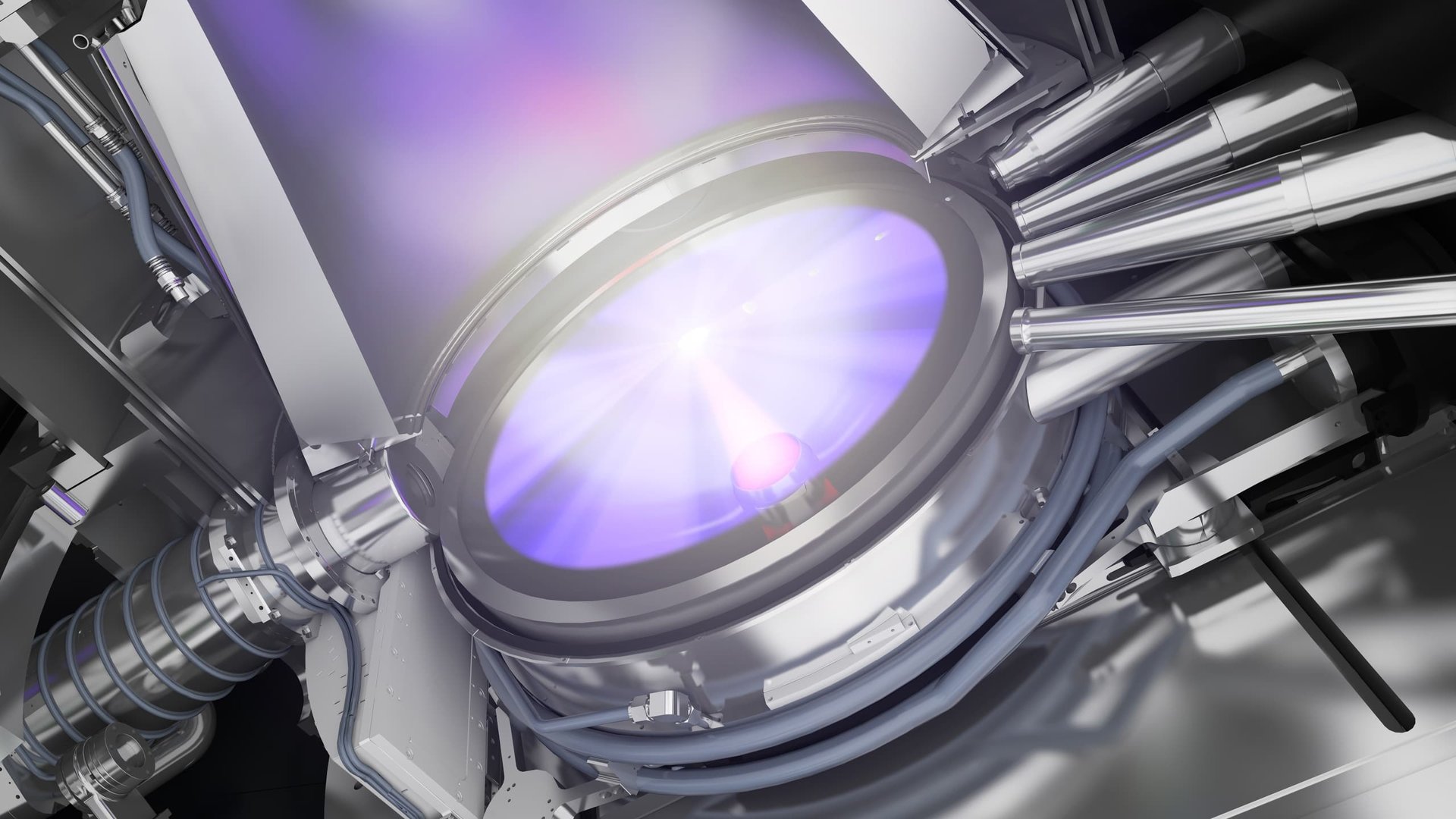
Doing so involves firing a drop of molten tin about the size of a grain of pollen. One laser pulse strikes to flatten it, then a second to create a plasma almost 40 times hotter than the sun’s surface. This then releases its energy as EUV light. The act repeats 50,000 times a second.
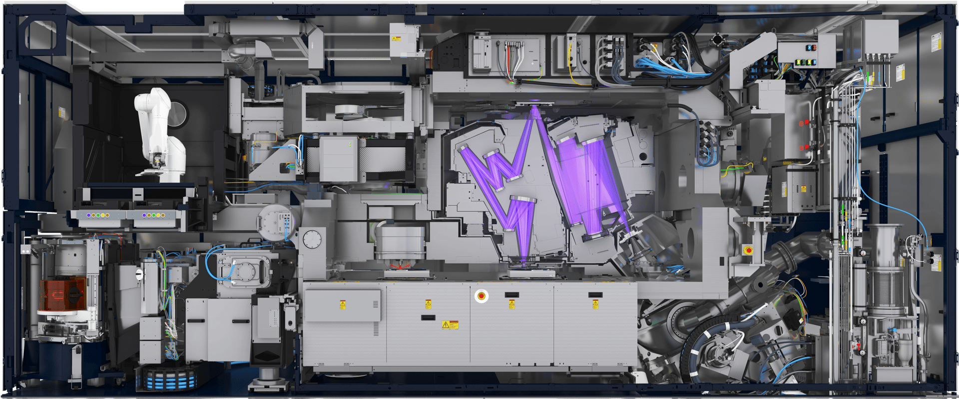
These light pulses are then focused using a series of the smoothest mirrors in the world. If you enlarged one to the size of Germany, the biggest surface bump would be 1mm high.
The ‘sharpened’ light enters a scanner where multilayer reflectors use ‘interference’ to create a deformed version of the desired chip’s circuitry pattern. It’s deformed because the physical and chemical processes that follow cause distortions. So adjustments are made based on readings taken from the EUV machine and test wafers.
After the scanner, the light bounces across more mirrors to shrink the pattern by a factor of four before reaching a silicon wafer coated in a light-sensitive film. The machine checks the wafer’s position and adjusts it 20,000 times a second. It cannot be more than half an atom off-place for each exposure.
This extraordinary level of precision is required because each wafer must be etched, filled with copper, polished, covered in a new silicon layer and film and then returned for a follow-up lithographic exposure up to 100 times before the chip is complete.
As if that doesn’t sound arduous enough, ASML must deal with the fact that everything absorbs EUV light – even air. So the light and everything it interacts with are contained in a vacuum.

ASML’s EUV machines feature hundreds of thousands of components © ASML
It took ASML decades of work and billions of dollars of investment to create a commercial EUV machine.
The machines contain so many parts that it takes four jumbo jets to transport them to clients, where ASML staff assemble them into a box about the size of a double-decker bus.
The firm also developed specialist software to measure and compensate for minuscule flaws. These result from tiny temperature and atmospheric pressure variations, which are impossible to avoid.
Chief executive Peter Wennink says that light wavelengths have historically had lithographic lifespans of 10 to 15 years. And the firm expects to be able to deliver meaningful improvements to its EUV machines until at least 2035.
These include debuting a higher-resolution EUV process in 2025 called high-numerical aperture (High-NA). It will involve a bigger machine whose parts must meet even more exacting standards. All of ASML's existing customers have submitted orders for High-NA.
One challenge that still needs to be addressed is that EUV machines are more energy intensive than their predecessors.
Apple has pledged to have a ‘net zero supply chain’ by 2030. As one of the biggest customers for state-of-the-art chips, that puts ASML under pressure to minimise the environmental impact of its next-generation equipment.
ASML’s market
ASML’s annual report for 2021 stated sales of 42 EUV systems, in addition to 267 less-advanced lithography machines (it competes with Nikon and Canon for DUV-based units).
Chip foundries typically require up to 18 EUV machines, each costing about €160m ($153m). The High-NA follow-ups will cost nearly double that amount.
A simplified guide to chip manufacturing
1. Wafers cut out of sausage-shaped crystal and polished to obtain a smooth surface
2. Thin films of material deposited on wafer and coated with a light-sensitive photoresist
3. DUV or EUV lithography creates chip patterns in the photoresist layer
4. ‘Etch’ bakes and develops the wafer and removes some of the photoresist
5. Electrically charged ions are directed into the exposed patterns to create transistors
6. Remaining photoresist removed
7. Process is repeated dozens of times to build up different layers of structure
8. Diamond saw cuts wafer into individual ‘dies’
9. Die placed onto a substrate base and covered with ‘heat spreader’ lid to create chip

As the global chip shortage demonstrates, rising demand for high-end semiconductors outstrips their supply.
But ASML and its key clients – TSMC, Samsung Foundry and Intel – are cautious.
It typically takes about 18 months for an EUV machine to come online after a manufacturer orders it. And the industry has repeatedly suffered cycles in which tight demand for chips has been followed by a glut of product, forcing prices down for all involved.
That was the case in the early 2000s when ASML’s shares suffered a 90 per cent peak-to-trough drop, and again in 2018 when its stock tumbled over 30 per cent.

Source: Eikon Datastream and Baillie Gifford & Co
However, ASML believes it is entering a period of sustained demand growth. The graph above illustrates that as of September 2022, the shares had made a total return of over 30,000 per cent, including dividends, since IPO. And while a ‘this time it’s different’ mindset should always inspire wariness, the company makes a convincing case.
Wennink notes that chip demand primarily depended on sales of PCs, smartphones and other consumer electronics during past cycles. While these still account for about half the market, the CEO says the long-term ‘megatrends’ driving growth are broader:
The automotive market
Cars can contain up to 3,000 microchips. They control everything from the infotainment and fuel-saving systems to security and automatic braking. Electric cars use more chips than their combustion engine counterparts. And the addition of advanced driver-assist and self-drive features should fuel further demand, particularly for components that draw lower battery power.
The green energy transition
Solar panels, wind turbines, hydrogen electrolysers, heat pumps and battery systems all need chips. So too do the computers required to monitor energy transmission and distribution. They take on a more significant role in a system with more intermittent and decentralised sources of energy generation.
High-performance computing applications
Creating virus vaccines, developing video games and simulating climate change are among the complex tasks that benefit from increased processing power and lower energy demand. More broadly, as more industries turn to artificial intelligence, data centres packed with powerful computer servers are required to train the models involved.
Internet of things
More objects are fitted with sensors, power management units and actuators (machine parts that control movement) and connect to the internet – all of which require chips. The data gathered allows more informed decisions and ‘smart’ features to be added, including voice controls and autonomous responses to changes in their environment.
A further factor in ASML’s favour is that the US and EU have woken up to the geopolitical risk of 80 per cent of the world’s semiconductor manufacturing capacity being in Asia.
The US’s recent CHIPS and Science Act includes $52bn of funds to boost domestic semiconductor manufacturing, while the proposed EU Chips Act aims to provide about €15bn ($16bn) of extra spending by 2030. Much of this will likely go to new foundries that will become customers of ASML’s machines.
Threats
ASML has many factors in its favour, but there are some ‘bear case’ considerations to keep in mind. Below are the most critical:
Rising input costs
The firm is dealing with two types of inflation. First, higher material and transport costs are driving up the cost of the third-party components it relies on. Second, it is increasing its headcount during tight demand for those with semiconductor skills.
These issues have already contributed to a squeezing of its gross margins. They have shrunk from about 53 per cent in 2021 to a forecast of “approaching 50 per cent” in 2022.
However, the firm’s lack of competition should help it pass these costs on to its clients over time. It has said that discussions are underway, and it expects gross margins to grow to between 56 to 60 per cent by 2030.
A China trade ban
In 2019, the US Government pressed the Netherlands to prevent ASML from selling its EUV equipment to Chinese chip makers. However, the firm continued to sell its DUV machines to the sector.
In October 2022, Washington imposed far-reaching export controls on China’s semiconductor industry. At the time of writing, ASML said it believed the direct impact to its business would be “fairly limited” and that it could “continue to ship non-EUV lithography tools out of Europe and into China”.
Chinese-based facilities run by either domestic or foreign companies made up nearly 15 per cent of ASML’s revenue in 2021, according to Bloomberg data.
The high costs of EUV
ASML believes that High-NA will enable it to shrink transistors to 1.5nm and beyond. But the €300m-plus cost of the next-generation machines may encourage chip designers to seek alternatives.
One trend is to increase the physical dimensions of a chip, whether created as a whole or out of multiple interconnected ‘chiplets’. However, this reduces the number of processors made from each wafer and increases the failure rate, driving up costs. Moreover, larger chips need more space inside computers, limiting how big they can realistically become.
Another trend is to stack transistors on top of each other in ‘3D designs’ to achieve greater densities without shrinking their size. This can be done using equipment made by ASML’s rivals. However, over time, more layers will be needed to match the speed increases EUV can deliver, driving up manufacturing costs. Eventually, switching to ASML’s equipment should become more cost-effective.
Emergence of a competitor
ASML’s last annual report flagged concerns that a Chinese company specialising in products to improve chip yields had potentially infringed its intellectual property. So the issue of IP theft is more than theoretical.
But the threat to its principal business is limited. Even if another company obtained a copy of the blueprints for its EUV machines, they would still need to replicate the embedded software that runs them. ASML has spent three decades developing the millions of lines of code involved in controlling the machines and positioning the silicon wafers at speed to high precision.
And even if this software were cloned, there’s still the matter of ASML harnessing a vast supply network of about 4,700 companies, one of which – the mirror maker Carl Zeiss SMT – it has a large minority stake in.
Others are working on alternative lithographic technologies, including electron beam, nanoimprinting and X-ray. However, we don’t expect them to achieve EUV’s throughput and scale in the foreseeable future.
Conclusion
ASML holds a unique position in the semiconductors ecosystem that is unlikely to change soon.
The industry has been prone to times of drought and glut. But there are reasons to think technological trends and geopolitical concerns will break this cycle, at least in the medium term. And for now, the firm says it is in the favourable position of demand significantly exceeding supply.
Baillie Gifford has a long history with the firm. We first invested in 1996, although there was a period in the mid-2000s when we weren’t a shareholder. We appreciate the far-sighted care it takes over its staff, suppliers and customers.
For instance, as the only EUV machine maker, it could push its prices much higher for short-term gain. However, its leaders are more focused on maximising value over the long term, which we believe is the better route to sustainable growth.
ASML can justly claim to be a critical contributor to the further speeding up of affordable computing power. And the only serious competition it faces comes from the laws of physics.
In our view, that puts it in a strong position to deliver solid returns for many years.
Risk Factors
The views expressed should not be considered as advice or a recommendation to buy, sell or hold a particular investment. They reflect opinion and should not be taken as statements of fact nor should any reliance be placed on them when making investment decisions.
This communication was produced and approved in December 2022 and has not been updated subsequently. It represents views held at the time of writing and may not reflect current thinking.
This communication contains information on investments which does not constitute independent research. Accordingly, it is not subject to the protections afforded to independent research, but is classified as advertising under Art 68 of the Financial Services Act (‘FinSA’) and Baillie Gifford and its staff may have dealt in the investments concerned.
All information is sourced from Baillie Gifford & Co and ASML and is current unless otherwise stated.
The images used in this communication are for illustrative purposes only.
Important Information
Baillie Gifford & Co and Baillie Gifford & Co Limited are authorised and regulated by the Financial Conduct Authority (FCA). Baillie Gifford & Co Limited is an Authorised Corporate Director of OEICs.
Baillie Gifford Overseas Limited provides investment management and advisory services to non-UK Professional/Institutional clients only. Baillie Gifford Overseas Limited is wholly owned by Baillie Gifford & Co. Baillie Gifford & Co and Baillie Gifford Overseas Limited are authorised and regulated by the FCA in the UK.
Persons resident or domiciled outside the UK should consult with their professional advisers as to whether they require any governmental or other consents in order to enable them to invest, and with their tax advisers for advice relevant to their own particular circumstances.
Financial Intermediaries
This communication is suitable for use of financial intermediaries. Financial intermediaries are solely responsible for any further distribution and Baillie Gifford takes no responsibility for the reliance on this document by any other person who did not receive this document directly from Baillie Gifford.
Europe
Baillie Gifford Investment Management (Europe) Limited provides investment management and advisory services to European (excluding UK) clients. It was incorporated in Ireland in May 2018. Baillie Gifford Investment Management (Europe) Limited is authorised by the Central Bank of Ireland as an AIFM under the AIFM Regulations and as a UCITS management company under the UCITS Regulation. Baillie Gifford Investment Management (Europe) Limited is also authorised in accordance with Regulation 7 of the AIFM Regulations, to provide management of portfolios of investments, including Individual Portfolio Management (‘IPM’) and Non-Core Services. Baillie Gifford Investment Management (Europe) Limited has been appointed as UCITS management company to the following UCITS umbrella company; Baillie Gifford Worldwide Funds plc. Through passporting it has established Baillie Gifford Investment Management (Europe) Limited (Frankfurt Branch) to market its investment management and advisory services and distribute Baillie Gifford Worldwide Funds plc in Germany. Similarly, it has established Baillie Gifford Investment Management (Europe) Limited (Amsterdam Branch) to market its investment management and advisory services and distribute Baillie Gifford Worldwide Funds plc in The Netherlands. Baillie Gifford Investment Management (Europe) Limited also has a representative office in Zurich, Switzerland pursuant to Art. 58 of the Federal Act on Financial Institutions (“FinIA”). The representative office is authorised by the Swiss Financial Market Supervisory Authority (FINMA). The representative office does not constitute a branch and therefore does not have authority to commit Baillie Gifford Investment Management (Europe) Limited. Baillie Gifford Investment Management (Europe) Limited is a wholly owned subsidiary of Baillie Gifford Overseas Limited, which is wholly owned by Baillie Gifford & Co. Baillie Gifford Overseas Limited and Baillie Gifford & Co are authorised and regulated in the UK by the Financial Conduct Authority.
China
Baillie Gifford Investment Management (Shanghai) Limited 柏基投资管理(上海)有限公司(‘BGIMS’) is wholly owned by Baillie Gifford Overseas Limited and may provide investment research to the Baillie Gifford Group pursuant to applicable laws. BGIMS is incorporated in Shanghai in the People’s Republic of China (‘PRC’) as a wholly foreign-owned limited liability company with a unified social credit code of 91310000MA1FL6KQ30. BGIMS is a registered Private Fund Manager with the Asset Management Association of China (‘AMAC’) and manages private security investment fund in the PRC, with a registration code of P1071226.
Baillie Gifford Overseas Investment Fund Management (Shanghai) Limited
柏基海外投资基金管理(上海)有限公司(‘BGQS’) is a wholly owned subsidiary of BGIMS incorporated in Shanghai as a limited liability company with its unified social credit code of 91310000MA1FL7JFXQ. BGQS is a registered Private Fund Manager with AMAC with a registration code of P1071708. BGQS has been approved by Shanghai Municipal Financial Regulatory Bureau for the Qualified Domestic Limited Partners (QDLP) Pilot Program, under which it may raise funds from PRC investors for making overseas investments.
Hong Kong
Baillie Gifford Asia (Hong Kong) Limited 柏基亞洲(香港)有限公司 is wholly owned by Baillie Gifford Overseas Limited and holds a Type 1 and a Type 2 license from the Securities & Futures Commission of Hong Kong to market and distribute Baillie Gifford’s range of collective investment schemes to professional investors in Hong Kong. Baillie Gifford Asia (Hong Kong) Limited 柏基亞洲(香港)有限公司 can be contacted at Suites 2713-2715, Two International Finance Centre, 8 Finance Street, Central, Hong Kong. Telephone +852 3756 5700.
South Korea
Baillie Gifford Overseas Limited is licensed with the Financial Services Commission in South Korea as a cross border Discretionary Investment Manager and Non-discretionary Investment Adviser.
Japan
Mitsubishi UFJ Baillie Gifford Asset Management Limited (‘MUBGAM’) is a joint venture company between Mitsubishi UFJ Trust & Banking Corporation and Baillie Gifford Overseas Limited. MUBGAM is authorised and regulated by the Financial Conduct Authority.
Australia
Baillie Gifford Overseas Limited (ARBN 118 567 178) is registered as a foreign company under the Corporations Act 2001 (Cth) and holds Foreign Australian Financial Services Licence No 528911. This material is provided to you on the basis that you are a “wholesale client” within the meaning of section 761G of the Corporations Act 2001 (Cth) (“Corporations Act”). Please advise Baillie Gifford Overseas Limited immediately if you are not a wholesale client. In no circumstances may this material be made available to a “retail client” within the meaning of section 761G of the Corporations Act.
This material contains general information only. It does not take into account any person’s objectives, financial situation or needs.
South Africa
Baillie Gifford Overseas Limited is registered as a Foreign Financial Services Provider with the Financial Sector Conduct Authority in South Africa.
North America
Baillie Gifford International LLC is wholly owned by Baillie Gifford Overseas Limited; it was formed in Delaware in 2005 and is registered with the SEC. It is the legal entity through which Baillie Gifford Overseas Limited provides client service and marketing functions in North America. Baillie Gifford Overseas Limited is registered with the SEC in the United States of America.
The Manager is not resident in Canada, its head office and principal place of business is in Edinburgh, Scotland. Baillie Gifford Overseas Limited is regulated in Canada as a portfolio manager and exempt market dealer with the Ontario Securities Commission ('OSC'). Its portfolio manager licence is currently passported into Alberta, Quebec, Saskatchewan, Manitoba and Newfoundland & Labrador whereas the exempt market dealer licence is passported across all Canadian provinces and territories. Baillie Gifford International LLC is regulated by the OSC as an exempt market and its licence is passported across all Canadian provinces and territories. Baillie Gifford Investment Management (Europe) Limited (‘BGE’) relies on the International Investment Fund Manager Exemption in the provinces of Ontario and Quebec.
Israel
Baillie Gifford Overseas is not licensed under Israel’s Regulation of Investment Advising, Investment Marketing and Portfolio Management Law, 5755-1995 (the Advice Law) and does not carry insurance pursuant to the Advice Law. This material is only intended for those categories of Israeli residents who are qualified clients listed on the First Addendum to the Advice Law.


